Comparing DUV, EUV, and NIL Technologies: Which is Best for Semiconductor Manufacturing?
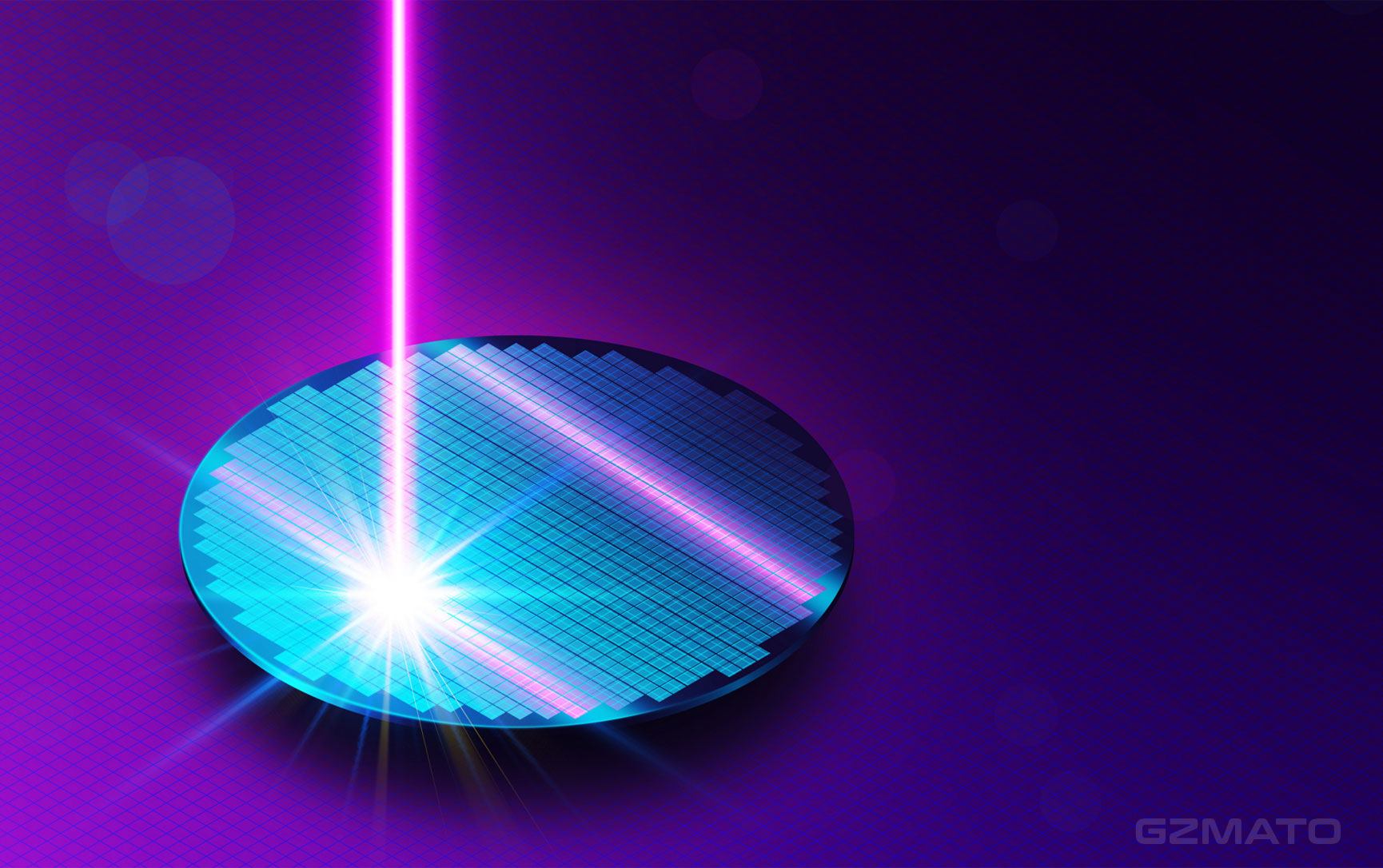
In the ever-evolving world of semiconductor manufacturing, achieving smaller, more powerful chips is a constant challenge. As semiconductor nodes shrink, lithography technologies—the processes used to etch intricate patterns onto silicon wafers—play a critical role in defining how efficiently chips can be produced. Among the leading technologies, Deep Ultraviolet (DUV), Extreme Ultraviolet (EUV), and Nanoimprint Lithography (NIL) stand out as key contenders. But when it comes to cutting-edge chip production, which is the best option for the future? Let’s dive into an analysis of each technology’s strengths, weaknesses, and suitability for different applications.
DUV: The Workhorse of Semiconductor Manufacturing
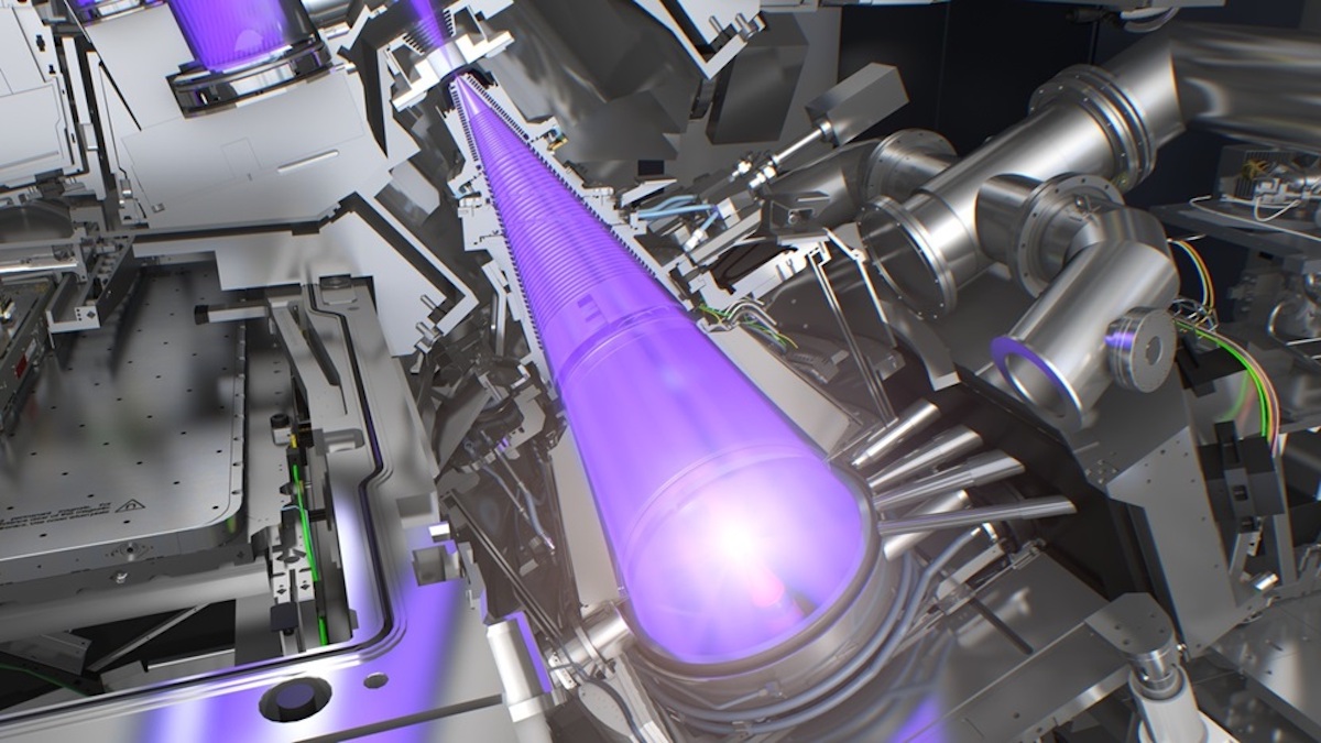
Deep Ultraviolet (DUV) lithography has been the backbone of semiconductor manufacturing for decades. DUV systems use light with wavelengths around 193 nm or 248 nm (depending on the laser used) to create patterns on semiconductor wafers. These systems have been integral to producing everything from microprocessors to memory chips, especially in older process nodes (e.g., 28nm, 14nm, 7nm).
Strengths of DUV:
- Maturity: DUV is a well-established technology with decades of use in the industry. There’s a deep understanding of its strengths and limitations, and it’s supported by a vast infrastructure of tooling and materials.
- Cost-Effective: DUV lithography tools are relatively less expensive compared to newer technologies like EUV. This makes it a popular choice for older semiconductor nodes and high-volume production where cost efficiency is key.
- High Throughput: DUV systems are designed for high throughput, meaning they can handle large volumes of wafers, making them ideal for mass production of mature chips.
Limitations of DUV:
- Resolution: DUV is limited by its longer wavelength (193nm or 248nm), making it difficult to print extremely small features. For smaller nodes (5nm or beyond), DUV needs to rely on multiple patterning techniques, which adds complexity and cost.
- Scalability: As chips shrink below 7nm, DUV struggles to meet the demands of smaller features without compromising yield, making it less suitable for the latest generations of chips.
EUV: The Future of Advanced Semiconductor Manufacturing
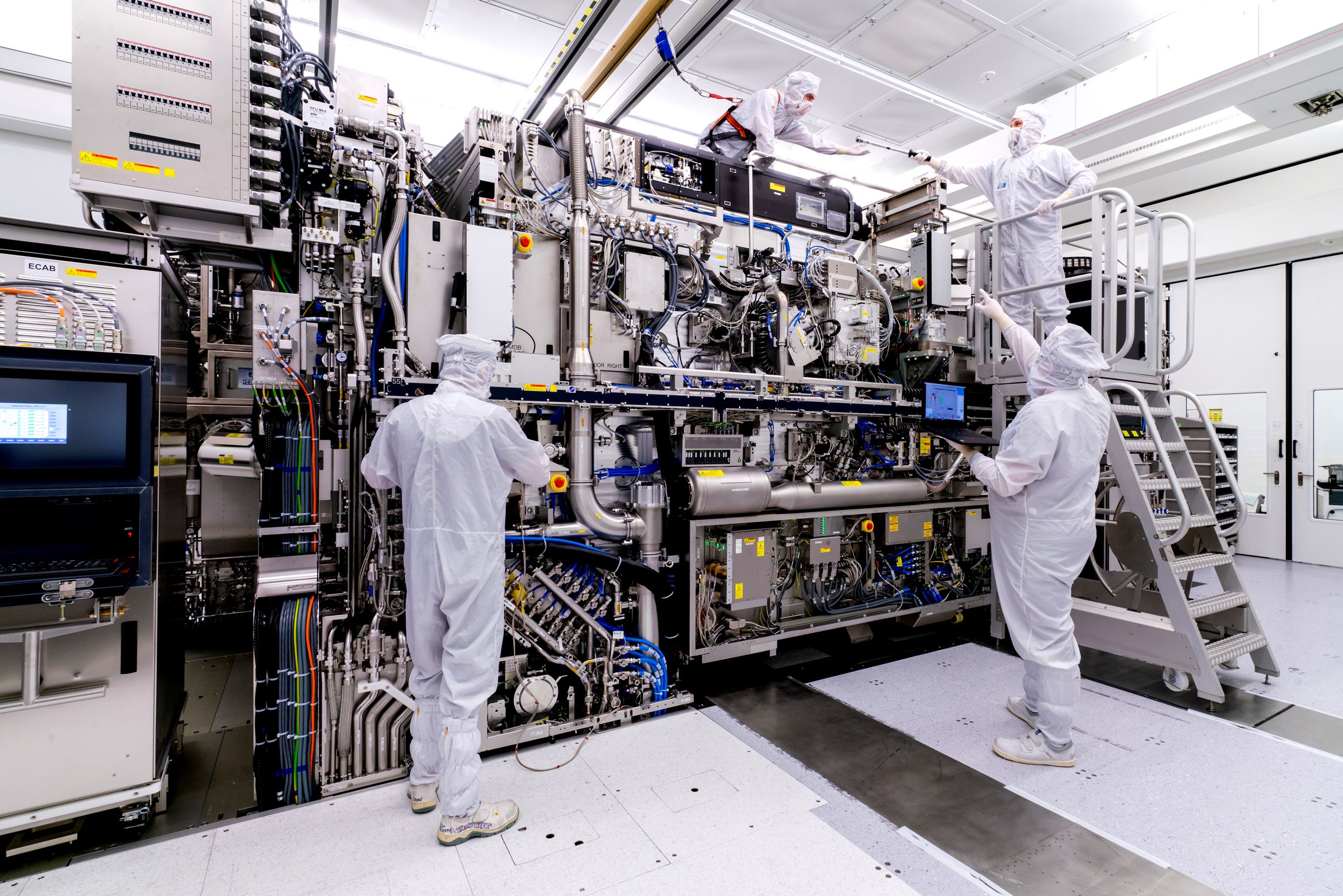
Extreme Ultraviolet (EUV) lithography represents the cutting-edge of semiconductor manufacturing. Operating at a shorter wavelength of 13.5 nm, EUV has been developed to address the challenges posed by smaller process nodes. It’s the key technology enabling the production of chips at 5nm, 3nm, and beyond.
Strengths of EUV:
- High Resolution: EUV’s shorter wavelength allows it to achieve significantly better resolution than DUV. This makes EUV the best choice for advanced semiconductor nodes like 5nm and 3nm, where smaller transistor features are essential for enhancing chip performance and efficiency.
- Single Exposure: Unlike DUV, which requires multiple patterning to create smaller features, EUV can print these fine features in a single exposure, reducing the complexity of the process and improving manufacturing efficiency.
- Enabling Future Chips: EUV is critical for the semiconductor industry to continue its progress toward the 2nm and 1nm nodes. Without EUV, the industry would struggle to keep pace with the demand for smaller, more powerful chips.
Limitations of EUV:
- Cost and Complexity: EUV machines are extremely expensive (over $150 million per system), and the process is complicated, requiring specialized light sources and reflective optics. This makes EUV a high-investment, high-risk technology.
- Lower Throughput: EUV systems currently have lower throughput compared to DUV, meaning fewer wafers can be processed per hour. This challenge is being addressed, but it still limits the scalability of EUV for mass production in some cases.
- Maturity: While EUV is rapidly advancing, it is still a relatively new technology. Issues like source power, mask defects, and resist development are ongoing challenges that need to be solved before EUV can truly scale to high-volume production.
NIL: The Emerging Contender in Nanoscale Fabrication
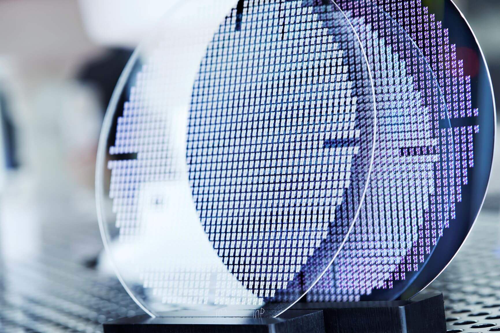
Nanoimprint Lithography (NIL) is an alternative lithography technology that uses a mold to imprint nanoscale patterns directly onto a wafer. Unlike traditional photolithography, NIL does not rely on light but instead employs mechanical pressing to transfer patterns, which can result in extreme precision and small feature sizes.
Strengths of NIL:
- Sub-10nm Resolution: NIL can achieve ultra-high resolution at the nanoscale—potentially even sub-10nm, which makes it an excellent option for highly intricate patterns.
- Cost-Effective for Niche Applications: For certain specialized applications, such as biomedical devices, quantum computing, and photonic devices, NIL can be a more cost-effective solution than EUV or DUV due to its relatively simple process.
- No Need for Expensive Optics: Unlike EUV, NIL doesn’t require expensive optical systems or light sources. This can make it a more accessible and scalable option for smaller-scale or niche manufacturing.
Limitations of NIL:
- Scalability: NIL has not yet reached the same level of scalability as DUV and EUV for mass production of advanced semiconductor chips. While it can produce fine features, the process can be slow, and uniformity across large wafers remains a challenge.
- Maturity: While NIL has shown promise in research and development, it is still an emerging technology and not yet widely adopted for mainstream semiconductor manufacturing.
- Pattern Transfer Issues: NIL faces challenges with defectivity and pattern transfer onto large-area wafers, especially for large-scale production.
Which Technology is Best?
Choosing the best lithography technology depends on the application:
- For Advanced Node Chips (5nm and Beyond): EUV is the clear winner. It’s currently the only technology capable of achieving the resolution required for these advanced process nodes. While expensive and complex, EUV is necessary for the semiconductor industry to continue pushing the limits of chip miniaturization and performance.
- For Mature Nodes (Above 7nm): DUV remains the most practical choice. It offers a mature, cost-effective solution for producing chips at older nodes. Although DUV has limitations at the smallest process nodes, it remains highly effective for the majority of the semiconductor market.
- For Niche Applications in Nanoscale Manufacturing: NIL shows potential in areas where extreme precision is required, such as biotech, photonics, and advanced packaging. While NIL isn’t yet ready for large-scale semiconductor production, it could be the go-to choice for specialized industries requiring high-density, small-scale patterns.
Conclusion
The choice between DUV, EUV, and NIL is not straightforward—each has its own set of strengths, limitations, and use cases. EUV is indispensable for pushing the boundaries of semiconductor technology at the most advanced nodes, while DUV continues to dominate in older nodes where cost and throughput are the primary concerns. NIL, though still emerging, could provide a breakthrough for highly specialized applications that demand extreme resolution.
As the semiconductor industry continues to evolve, it will likely rely on a combination of these technologies, choosing the right one based on the needs of each specific manufacturing process. For now, EUV is firmly at the forefront of advanced manufacturing, but the future may hold even more exciting developments for NIL as the technology matures.
What is Nanoimprint Lithography (NIL)?
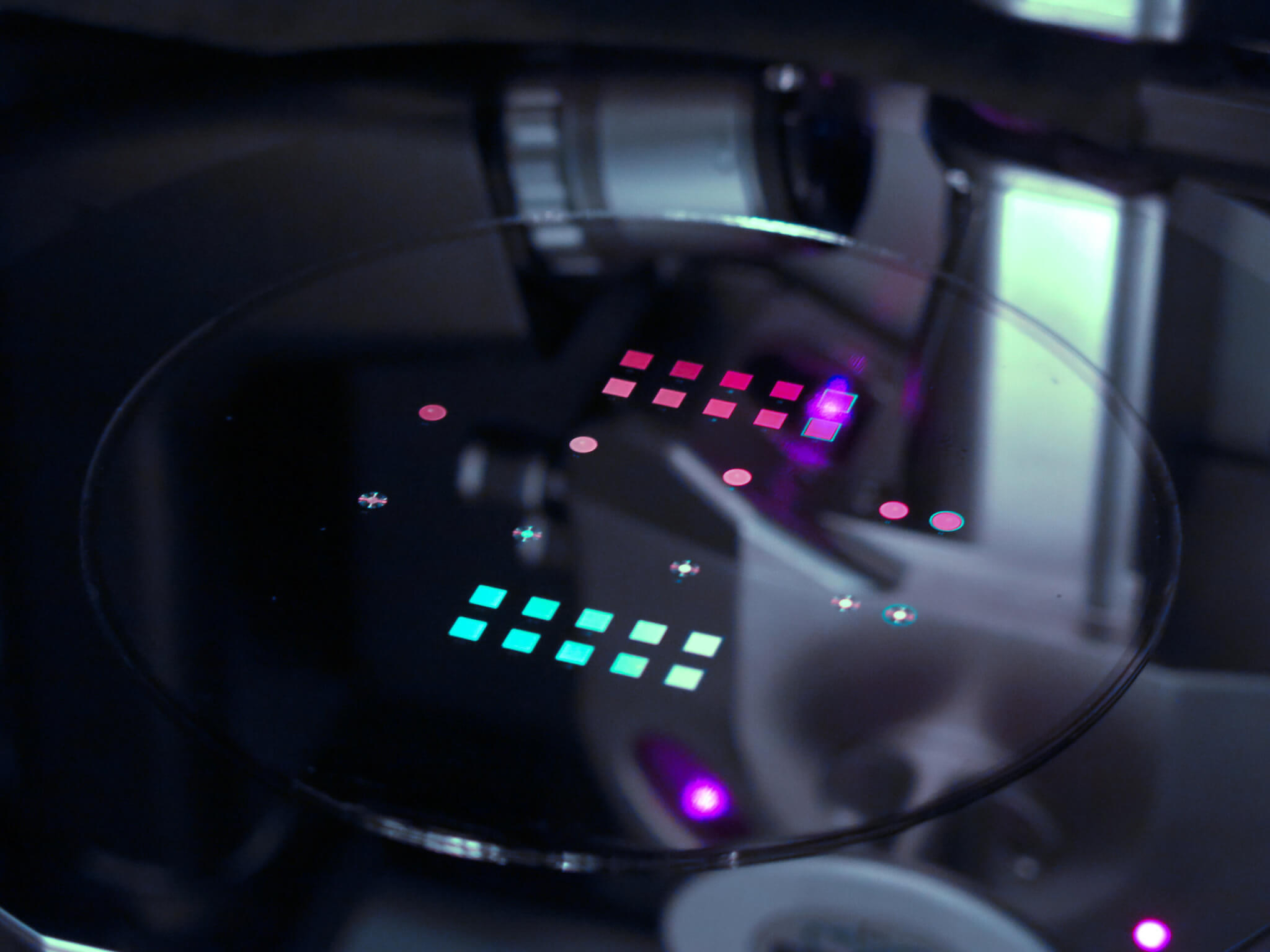
Nanoimprint Lithography (NIL) is a nanofabrication technique used to create extremely fine patterns on a substrate, typically at the nanoscale. Unlike traditional photolithography, which uses light to etch patterns onto a wafer, NIL employs a mechanical process to directly imprint patterns using a mold. This technique can achieve resolutions in the sub-10nm range, which is crucial for the development of next-generation semiconductor devices and other nanoscale applications.
The basic process of NIL involves pressing a mold with nanoscale patterns onto a layer of resist material on the substrate. The resist material, which can be either thermal or UV curable, flows into the mold cavities. After imprinting, the resist is either cured or hardened, and the mold is removed, leaving behind the patterned structure on the substrate.
Key Types of NIL
There are several variations of NIL, each with its own advantages and applications:
- Thermal NIL (T-NIL):
-
- Principle: In thermal NIL, the resist material is heated above its glass transition temperature (Tg). The mold is then pressed onto the resist at high temperatures, allowing the material to flow into the mold’s cavities.
- Advantages: Thermal NIL offers high pattern fidelity and can be used for a wide range of materials.
- Disadvantages: The heating process can limit the speed of production and introduce potential thermal stress on the substrate.
- UV NIL (UV-NIL):
-
- Principle: In UV NIL, the resist is UV-sensitive, and UV light is used to cure the resist after imprinting. The mold is pressed onto the resist material, which is then exposed to UV light to solidify the pattern.
- Advantages: UV NIL can be faster than thermal NIL due to the use of UV curing, making it potentially more suitable for high-throughput applications.
- Disadvantages: The resolution can sometimes be limited by the UV resist material’s properties and curing speed.
- Roll-to-Roll NIL:
-
- Principle: In this variant, the process is applied in a continuous roll-to-roll format, where a flexible substrate (such as plastic) is imprinted in a continuous, high-throughput manner.
- Advantages: This method is well-suited for large-scale production of flexible electronics and sensors.
- Disadvantages: It may not be as effective for rigid semiconductor manufacturing due to challenges in maintaining uniformity and precision across the roll.
Key Advantages of NIL Technology
- High Resolution:
-
- Unmatched Precision: NIL can achieve extremely fine resolutions, often sub-10nm, thanks to the mechanical process of imprinting patterns directly. This is far beyond the capabilities of conventional photolithography techniques like DUV and EUV.
- Fine Patterning: NIL is capable of creating very fine nanostructures, which are ideal for applications in fields like nanoelectronics, biotechnology, and photonics.
- Cost-Effective:
-
- Lower Tooling Costs: Compared to EUV, NIL is less expensive in terms of capital equipment costs. It doesn’t require complex optics or light sources, which significantly reduces the price of production tools.
- Simpler Process: NIL’s simpler process, compared to photolithography, avoids many of the high costs associated with conventional photomasks and light sources.
- High Throughput Potential:
-
- While NIL has been slower to scale than DUV and EUV in mass production, its high throughput potential in certain applications—such as mems (microelectromechanical systems), flexible electronics, and displays—is notable. Variants like roll-to-roll NIL promise continuous production, increasing efficiency in specific markets.
- Patterning of Complex 3D Structures:
-
- NIL can be used to create 3D nanostructures, which is particularly useful for applications in nanophotonics, optical devices, and microfluidics. Its ability to create intricate patterns on surfaces opens up new opportunities in biosensing and drug delivery systems.
- Flexibility for Various Substrates:
-
- Unlike photolithography, which is often limited to specific materials (typically silicon), NIL can be used on a variety of substrates—including metals, polymers, and even flexible materials like plastic or glass. This makes NIL attractive for a wide range of industries.
Applications of NIL
NIL is particularly well-suited for nanoscale manufacturing, where high precision is needed but traditional photolithography techniques may not be effective. Some prominent applications include:
1. Semiconductor Manufacturing:
-
- While NIL is not yet widely used for mainstream semiconductor production, it holds promise for next-generation nodes and specific nanoscale patterning tasks, especially for advanced memory devices, quantum computing, and optical devices.
2. Photonic Devices:
-
- NIL is ideal for creating nanophotonic structures, such as waveguides, metamaterials, and photonic crystals. Its high resolution makes it an excellent choice for optical communications, laser technologies, and light-emitting diodes (LEDs).
3. Flexible Electronics:
-
- NIL's ability to imprint patterns on flexible substrates (using roll-to-roll NIL) makes it well-suited for the production of flexible circuits, displays, sensors, and other wearable electronics.
4. Bioelectronics and Sensors:
-
- NIL is used in creating biosensors, lab-on-chip devices, and microfluidic systems. Its ability to create precise patterns allows for high-density molecular detection or for applications in drug delivery and diagnostics.
5. Optical Lithography for Large Area Manufacturing:
-
- NIL can also be used in the production of large-area devices, such as LCDs and OLED displays, due to its capability to pattern large substrates efficiently.
Challenges and Limitations of NIL
Despite its impressive capabilities, NIL faces several challenges, particularly in terms of scalability and integration into high-volume manufacturing processes.
- Defectivity:
-
-
-
- One of the primary challenges with NIL is the potential for defects during the imprinting process. Variations in mold alignment, pressure, or material flow can result in defects in the pattern, which could affect the yield of devices.
-
-
-
- Throughput for Mass Production:
- Although NIL has high throughput potential for specific applications, the imprinting speed may not yet match that of more established techniques like DUV and EUV for high-volume semiconductor production. As a result, it is still not widely used for mainstream manufacturing of advanced chips.
- Mold Fabrication:
- Fabricating the molds for NIL can be complex and time-consuming, especially for extremely fine patterns. The mold's quality directly impacts the final pattern resolution, and defects in the mold can propagate throughout the entire wafer.
- Pattern Transfer Issues:
- Achieving uniformity in pattern transfer across the entire wafer can be a challenge, especially for large-scale production. Ensuring that patterns are consistently transferred across large areas without distortion remains an ongoing hurdle.
- Material Compatibility:
-
- While NIL works on a variety of materials, not all resists or substrates are ideal for the process. Researchers are continually working on developing better resist materials that can withstand the high pressures of imprinting while maintaining excellent pattern fidelity.
The Future of NIL Technology
Nanoimprint Lithography is poised to make significant strides in the coming years, particularly in niche markets that demand high precision and small features. It could be a game-changer in fields like biotechnology, nanophotonics, and flexible electronics, where traditional photolithography struggles to meet the requirements for resolution and material diversity.
However, for mainstream semiconductor manufacturing, NIL still has work to do. Challenges like defectivity, scalability, and tool integration must be addressed before NIL can compete with EUV and DUV in high-volume production of advanced semiconductor nodes (e.g., sub-5nm).
In summary, while EUV and DUV dominate the semiconductor manufacturing landscape today, NIL remains a promising technology for specialized applications that demand the highest level of precision and flexibility. As research continues, NIL may one day complement or even surpass photolithography in specific sectors.
Source: ChatGPT